

Information Technology (IT) Pioneers
Retirees and former employees of Unisys, Lockheed Martin, and their heritage companies
Memory Engineering, Chapter 45
1. Introduction
Rotating Drum memories were the ERA entree into the computer world in that programs and data could be loaded thus saved when power was removed. These provided the technology baseline which eventually led to all rotating magnetic memories - including the PC hard drives. Even as the magnetic media and sensors were replaced with optical readers and media to create today's PC CDs, the rotation mechanisms and sensor proximities grew out of the ERA magnetic drum patents. We have three drums at the Lawshe Memorial Museum, described in a Larry Bolton paper and section 2 hereunder.
An early ERA patent agreement with IBM gave them a jump start for their 650 computer memory. Project Whirlwind at MIT used drum memories built by ERA. From the October 14, 1952 Orbit newsletter: "Kenneth MacVicar is here from MIT running acceptance tests on magnetic storage systems for MIT's project Whirlwind. J.J. O'Brien, Ed Rich, and Ben Morris of MIT were here earlier in the week.
The Mated Film memory was initially developed for the 1824 space borne computers. Then it wended its way into Navy computers and other products that needed fast memory. In the 80's, the original 1832 AN/AYK-10 computer's film memory was replaced with semi-conductor memory chassis. [lab]
Plated wire memories were used in the AN/UYK-10 computer {Minute Man Launch Control Facility processors}, in the commercial 9000 series, and 1110 series machines. The 1110 series eventually replaced the plated wire with semi-conductor memory modules. [lab]
2. Drum Memories
2.1 Development History
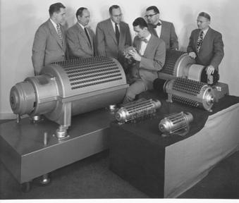 The
drum development engineers and management shown in this early 50's photo,
left to right are:
The
drum development engineers and management shown in this early 50's photo,
left to right are:
 William Keye, Arnold Hendrickson, Robert Perkins, Frank Mullaney, Dr.
Arnold Cohen, and John 'Jack' Hill.
Dr. Cohen and Sid Rubens are credited with patenting the rotating magnetic
drum. On the right is the installation of a drum into an early
110x computer.
William Keye, Arnold Hendrickson, Robert Perkins, Frank Mullaney, Dr.
Arnold Cohen, and John 'Jack' Hill.
Dr. Cohen and Sid Rubens are credited with patenting the rotating magnetic
drum. On the right is the installation of a drum into an early
110x computer.
We'd claim that this drum was the world's first computer 'hard drive' - the prototype description was presented as a paper in 1947. The paper's presenter, J. Coombs, left ERA to work for IBM in their drum development department.
The rotating drum technology allowed ERA to deliver
the world's first production stored-program computer* (ATLAS
- ERA 1101) to a customer site in October 1950. The engineers making
the installation delivery to the National Security Agency predecessor
were Frank Mullaney and Jack Hill. As shown in the photo at the left,
these drum products came in various sizes. They were first used in several
classified processors, then in the early 1100 computer series and
the UNIVAC SS-80 and SS-90 computers. The small drum in Mr.
Mullaney's hands was used in the 2052 project, an early airborne
computer, reference Chapter 57, AF
Computers.
Each of these early 'stored-program' machines was a one of a kind laboratory unit which used various volatile memory storage sections such as mercury acoustic delay lines. From a functional standpoint, these early memory technologies were akin to today's Random Access Memory - the contents are lost when power is turned off! The magnetic drum memory machines kept (stored) their programs when power was turned off, therefore did not have to be re-loaded time and again. The ERA ATLAS delivered into a customer's facility started the 1100 production series of commercial computers traceable to the UNISYS 2200 computer series of today. [LABenson]
*The ENIAC was modified in the spring of 1948, thus demonstrating stored-program concepts1 with a new control section. This was a couple of months before the British Manchester Baby that first ran a small demonstration program in June 1948. It was also before the BINAC in 1949.
1. IEEE Annals of the History of Computing - Volume 29, Number 4. 'ENIAC as a Stored-Program Computer: A New Look at the Old Records' by Crisin Rope.
2.2 Sesquicentennial Celebration display unit by Larry Bolton:
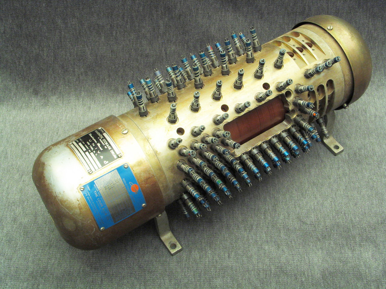 After many observations, counting, calculating, extrapolating, measuring,
etc. I have come up with a set of reasonable specs for the Harry Wise
model 1124G1 drum which we have had in our 2008 Capitol Mall and State
Fair exhibits.
After many observations, counting, calculating, extrapolating, measuring,
etc. I have come up with a set of reasonable specs for the Harry Wise
model 1124G1 drum which we have had in our 2008 Capitol Mall and State
Fair exhibits.
Capacity: 18.25K bytes
- Bit capacity: 146,000 bits
- Number of tracks: 133 (133 data heads present)
- Bits per track: 1100 (spec for the 1124 series and units with 4-3/8 drum)
- Tracks per inch (axial): 16 (as measured)
- Bits per inch (peripheral): 80 (same as all other drums)
- Drum diameter: 4-3/8 inch (as measured)
- Nominal RPM: 12,000 (as labeled)
- Motor Horsepower: 1/5 (as labeled)
- Weight: 80 lb (as measured)
- Dimensions: 7.5” H x 8.5” W x 22” L (as measured)
It has a Remington Rand New York label. The application for this drum is up for debate. Either a
special airborne application or a marketing demo have been proposed
so far. The heads and method of mounting them are of a variation we
have not seen in any photos of other drums of that period.
![]()
2.3 Minnesota Historical Society by Dick Lundgren:
This
circa 1946 magnetic drum from Engineering Research Associates (ERA)
is about to beat the cadence for our Legacy project as we roll into
2009.
 This drum is in the possession of the Minnesota Historical Society
(MHS), and it is soon to be featured as part of the MHS Greatest Generation
Exhibit which will open May 23, 2009 at the Minnesota History Center.
The drum is symbolic of local Minnesota industries which were started
in the early post-WWII days and grew to significance on the world scene.
This drum is in the possession of the Minnesota Historical Society
(MHS), and it is soon to be featured as part of the MHS Greatest Generation
Exhibit which will open May 23, 2009 at the Minnesota History Center.
The drum is symbolic of local Minnesota industries which were started
in the early post-WWII days and grew to significance on the world scene.
ERA, of course, grew and flourished under a sequence of familiar names, inter alia Remington Rand, Univac, Sperry, Unisys, and Lockheed Martin. Other local companies to be featured in the exhibit may include Honeywell, 3M, General Mills, and Medtronic.
 The ERA drum has sat untouched [and until
recently, underappreciated] for many years in basement storage at the
MHS. Under the guidance of Matt
Anderson, MHS curator for three dimensional objects. {Editor's
note: about 2013, Mr. Anderson moved to become curator at the Ford
Museum in MI.} The drum has
been restored to exhibit-quality status, and with help from Legacy personnel,
some missing hardware elements will be recreated. A photographic replica of this drum was a major attraction at
the display we developed for last year’s Sesquicentennial events.
The ERA drum has sat untouched [and until
recently, underappreciated] for many years in basement storage at the
MHS. Under the guidance of Matt
Anderson, MHS curator for three dimensional objects. {Editor's
note: about 2013, Mr. Anderson moved to become curator at the Ford
Museum in MI.} The drum has
been restored to exhibit-quality status, and with help from Legacy personnel,
some missing hardware elements will be recreated. A photographic replica of this drum was a major attraction at
the display we developed for last year’s Sesquicentennial events.
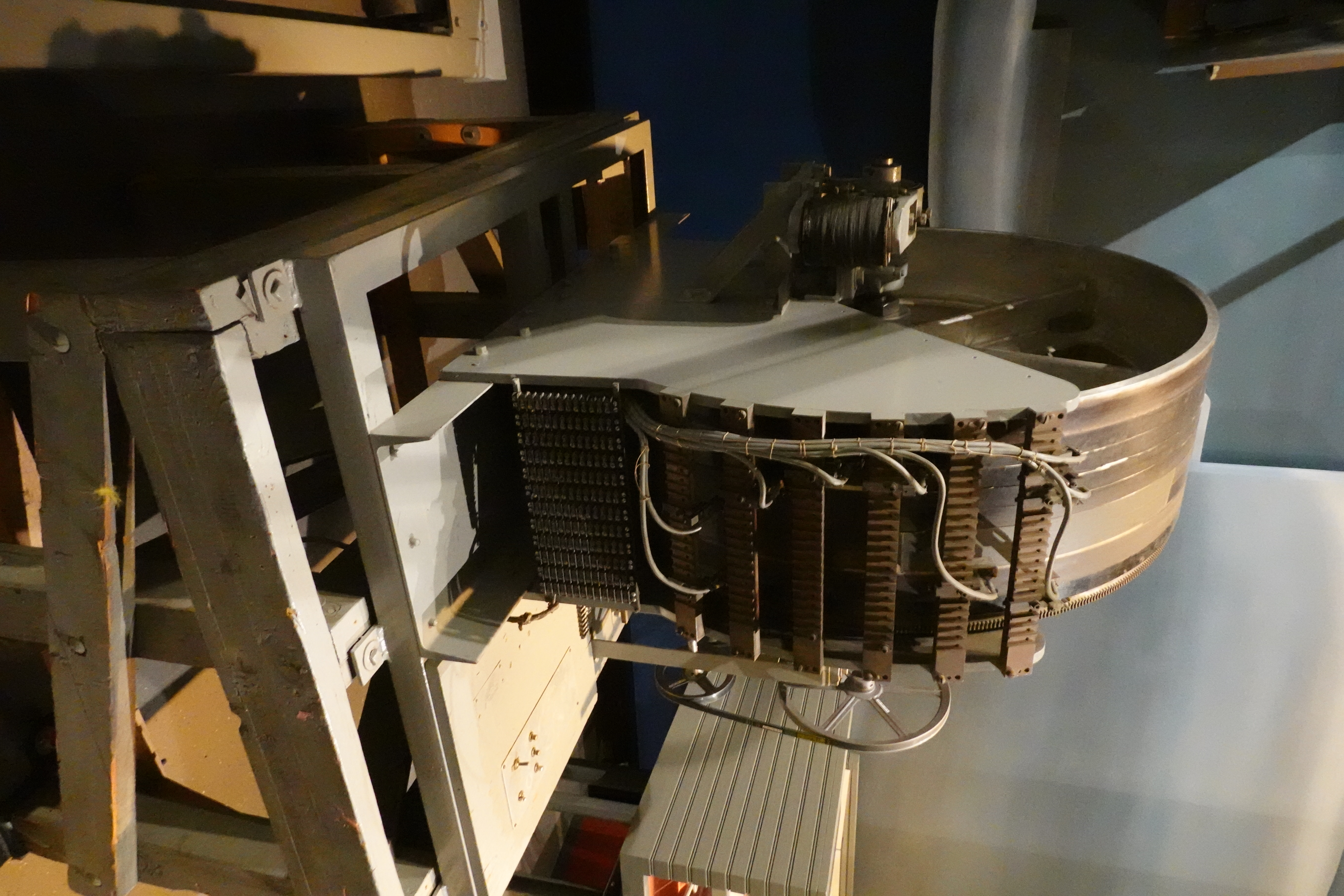
Unit Description by Don Weidenbach:
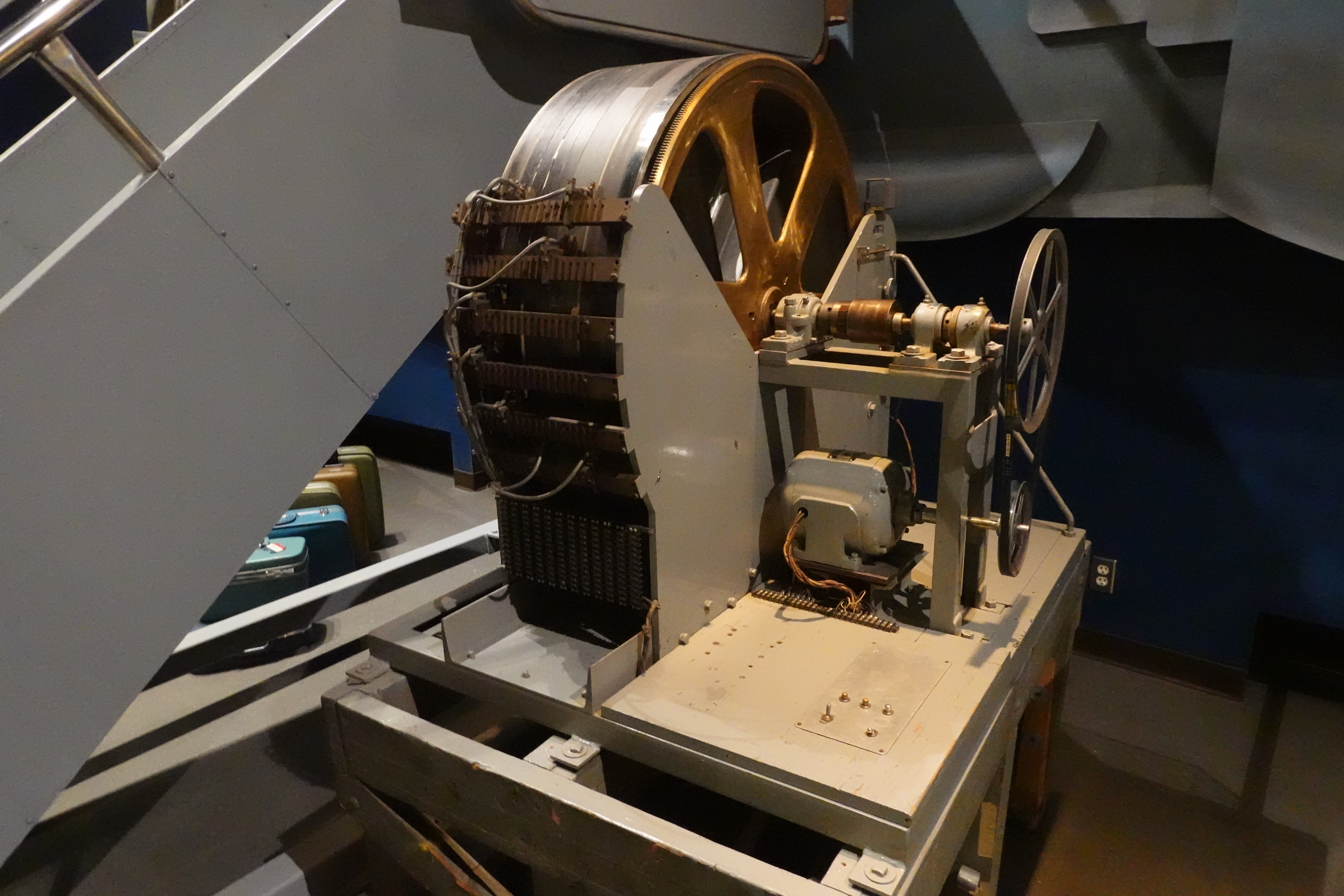
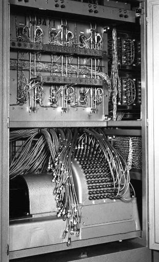
The drum; you asked about was the prototype for the Goldberg and Demon I computers. It was the first drum built at ERA, other than small lab-type "spinners" used for developing reading/recording circuits. The motor was coupled to the drum by pulleys and rubber V belts. The photo above shows a short shaft on the motor which does not extend out far enough to be in line with the drum shaft pulley, so it must have been extended somehow or purchased with a long shaft. The drum shaft is long because it has a magnetic clutch which disconnects the main motor from the drum when writing on the drum from a paper tape reader. This is done by a small worm gear motor [shown in the picture at the left]; moving the drum a step [or bit] at a time thru the large brass gear on the edge of the drum. The two driving systems are locked out by micro-switches so the drum can be driven by only one motor at any given time. The drive belts and pulleys were normally covered by a sheet metal shroud for obvious reasons.
I did not work on this prototype but did work on the production units
for both Goldberg and Demon and they very similar to this unit.
If you have further questions give me a shout. Don Weidenbach
{photos in this section taken by Keith Myhre, December
2021. More info at
Chapter 90, Exhibits. }
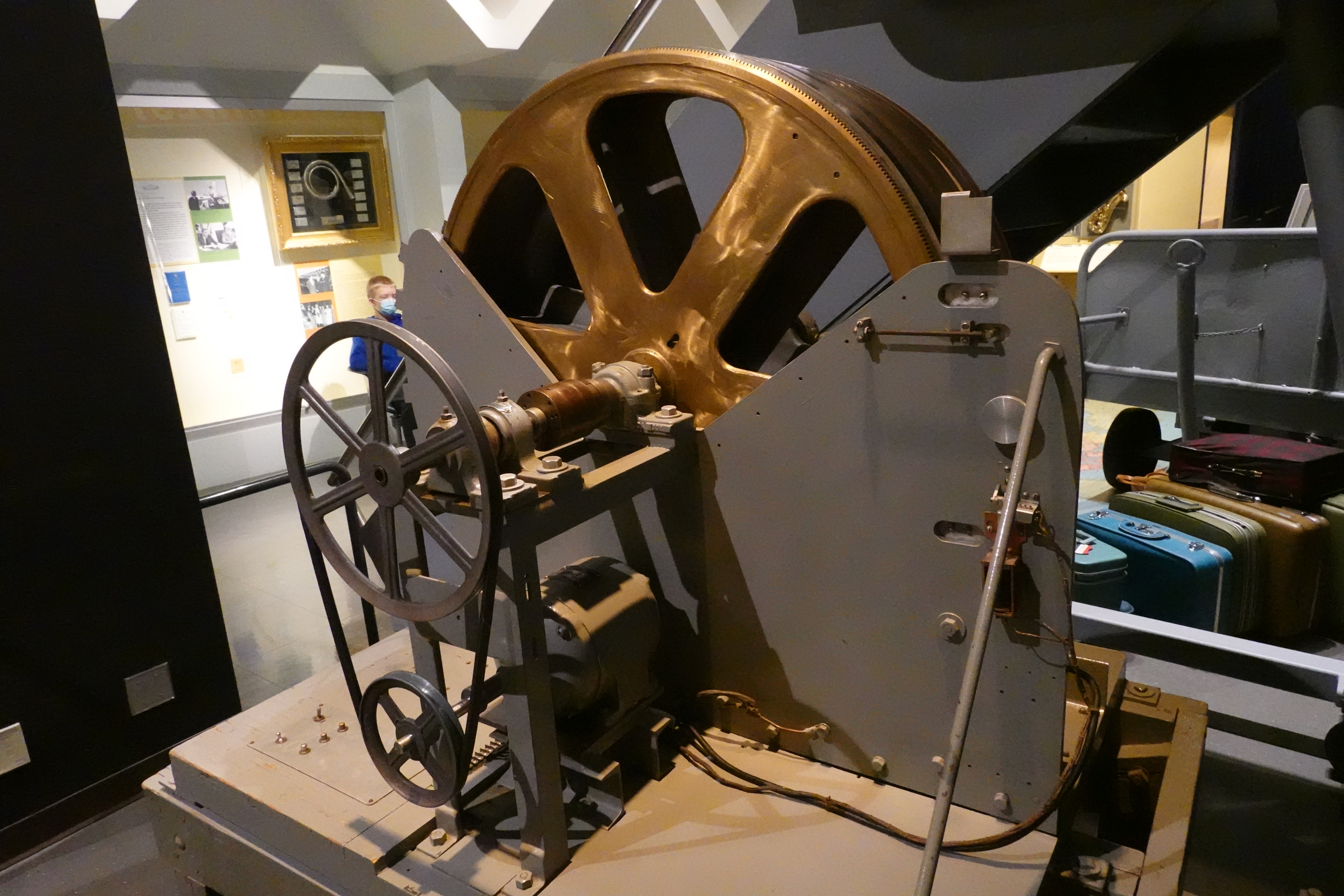
2.4 Fastrand Commercial Drums
Commercial drum memory units [FH-432, FH-880, and the Fastrand
series] were the mainstay for mass storage devices from the 60s
through the 70s before disc memories emerged.![]()
3. Braided Wire Memory by Jim Howe
I believe that the "braided
wire memory" was also known as the "Rope" memory. This memory was an
sort of an early PROM (~1966-1968), and was a configured as either 30
or 32 bits (depending on the application). 256 or 512 words - this
memory type served as the boot-strap memory for the CP-901 (original
P-C3 aircraft computer) and also for the original AN/UYK 7 computer.
The module was about ~4" x ~4" x ~0.6". The memory consisted of 30 or
32 ferrite cores (one core for each bit position), and either 256 or
512 magnet wires arranged in a diode selection matrix, one wire for
each word location.
Each of the ferrite
cores had about 30 turns of wire on it connected to the base-emitter
of a NPN transistor. A current pulse was driven down one wire to read
the data on that particular "word line". If the wire went through the
one of the cores, the corresponding transistor would turn ON, and that
bit would be read out as a "1". If the wire bypassed a core, the transistor
would remain off and that bit would be read as a "0". A loom was made
to string (i.e., program) the rope memory (the cores were physically
moved up or down to make "0's" or "1's" as the individual word lines
were pushed in a straight line through the mass of wires in the "rope"). The individual word line wires in the rope were terminated on printed
circuit boards inside of the rope module. [jh]
{Editor's Notes: Jim Howe's 'mechanical description' is quite accurate.
The wires going through or around the cores were about 40 gauge wire; 512
of these wires did look like a braided rope. I can vaguely remember
manually re-stringing a couple of word line wires to fix a problem with
an initial program. Sub-routines within the core-rope had to have
special entrance and exit method because the usual RJP (return jump
mnemonic) instruction could not store the 'came from' address as it
usually did in core memory.
I had not equated
the term 'braided wire' memory with the 'core rope' memory which was
used in the CP-901. The CP-901 had 512 words, not 256. These
512 words contained a paper tape bootstrap for diagnostic/test program
loading, an operational drum or magnetic tape loader, and a built in
self test [Start up diagnostics] program. I wrote the paper tape
loader, I believe that Jim Halvorson did most of the self test programming,
don't recall who wrote the magnetic tape and drum loader. There
was an original version for software development lab use then a production
version for use aboard the P-3C system. The diagnostic program
did a basic ISA check, an arithmetic section check, a registers test,
a simple bank 1 core memory test, then an output/input test using a
jumper cable from output channel 3 to input channel 6. If all of these
tests completed ok, about 90% of the CPU was functioning, 25% of the
core memory, and 1/16th of the I/O. If all of these core rope tests
completed, it was possible to load a more exhaustive set of tests from
magnetic tape/drum.
When we did developed
the 1830B for the German Navy's Fast Patrol Boat program, the core rope
program was updated to load from the 1840 Magnetic Tape Unit.
The designed in diagnostic program was tweaked for the other minor design
changes from the CP-901.} [lab]
![]()
4. Plated Wire Memory by Larry Bolton, Clint Crosby, and Jim Howe
This is a separate article document with a follow up addendum, focused on the defense systems use of this memory type in the Minute Man computers. Also, see an article from a Blue Bell manufacturing technician/engineer.
From Ron Q. Smith, April 17, 2018:
The 1110 used plated-wire memory for what was called “primary
memory.”
When the 1110 was begun, UNIVAC was expecting a major improvement in
manufacturing costs for plated-wire memory.
The 1110 was the first 1100 system designed to permit up to
16 million 36-bit words of memory. Early in the design of the 1110, they realized that
plated-wire memory was going to remain extremely expensive. As a result, they modified the 1110 to have two levels of
directly addressable memory. Primary memory would be plated wire but was limited to 262KW. Secondary memory was bulk core memory which could be up to
1MW in size. While the architecture permitted 16MW total, that size wasn’t actually
designed into the 1110.
The original idea was that the plated-wire memory would be used as a software-managed cache for the bulk
storage of secondary memory. The original plans called for a special “block transfer” box
that software could use to quickly move data and instructions between primary and secondary memory. Part way into the design of that, they realized that it would
as expensive as an instruction processor and not noticeably faster. So, they instead designed for up to 6 IPs. When we got the 1110 to start testing, it became obvious that
it took too much time to move data between memories – and the
secondary memory was directly addressable anyway. So, the software tried to keep only the most frequently used stuff in
primary and leave the rest in secondary. Usually that meant keeping instruction banks in primary and
data banks in bulk core. In the later release called the 1100/40 primary memory remained plated
wire, but secondary memory became semiconductors.
From Ian Eperson, January 2, 2020: I wonder if the VIP club is still in touch with the plated wire veterans - Larry Bolton, Clinton Crosby, James Howe...As a fellow veteran (though on the other side of the Atlantic) I was wondering if Univac only ever used non-destructive read wire. The answers are Yes to both questions. We have document the communications of several people as #265 of of Our Stories, Plated Wire Dialogues.
5. Bubble Memory by Lowell Benson
Bubble Memory devices were
sort of a competitor with the MNOS devices being manufactured in our
Eagan Semi-conductor plant. Those MNOS devices were being used on an
Air Force project - perhaps Jim Inda could recall which.
Our first non-IRAD use of Bubble Memory devices was an experimental
full ATR unit which was built for the Naval Air Development Center at
Johnsville, PA..
 Roman Fedorak was the Government technology sponsor
and project monitor. Ray Hedin and Sam Meddaugh working for, then department
manager, Dennis Amundson were the engineering personnel on the project.
Roy Lecy was the Program Manager for NADC projects at that time. The
intent of this Government sponsored project was trying to find a solid
state replacement for the drum memories operating aboard the P-3C and
S-3A ASW systems aircraft.
Roman Fedorak was the Government technology sponsor
and project monitor. Ray Hedin and Sam Meddaugh working for, then department
manager, Dennis Amundson were the engineering personnel on the project.
Roy Lecy was the Program Manager for NADC projects at that time. The
intent of this Government sponsored project was trying to find a solid
state replacement for the drum memories operating aboard the P-3C and
S-3A ASW systems aircraft.
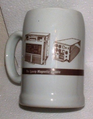 The souvenir mug shown here illustrates the ATR implementation
on the right. The left picture on the mug is the Coast Guard implementation,
a chassis modified from the AN/UYK-20 computer.
The souvenir mug shown here illustrates the ATR implementation
on the right. The left picture on the mug is the Coast Guard implementation,
a chassis modified from the AN/UYK-20 computer.
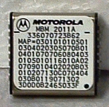
It was the NADC design baseline that won a contract with the Coast Guard
to provide a mass memory storage device for their patrol boats which
were beginning to implement a AN/UYK-20 Command and Control System.
The initial component used was the Motorola 1-megabit device show at
the right. There were a lot of quality control concerns during
the first ten units as Motorola struggled with their component manufacturing
processes. For the Coast Guard program, we delivered 26 units
over a two year period. Each unit had 16 array boards, each with eight
devices. Ray Hedin was the lead design engineer and checkout person
for the first three units as the build was transitioned from the Plant
8 prototype shop to Plant 1 manufacturing. P/N 7917502 4-megabit
bubble memory device specification for components made by Hitachi eventually
replaced the initial 1-Mbit Bubble Memory (chip) components
In June of 1984, Lowell Benson transferred from design engineering to Program Management to head-up the Coast Guard project. He replaced PM Roy Lecy to deal with the Motorola device manufacturing Quality Control problems. Shortly thereafter, there was a Program Management re-organization in which I reported to Marv Mirsch who was Director of Special Products. In the second production run, engineering made a few minor timing changes to facilitate device second sourcing from Hitachi.
As the Coast Guard 1st production run project was wrapping
up; I took on PM responsibility for the CIA's RISC chip development
project reporting to Neil Hahn. ![]() [lab]
[lab]
6. Film Memory
6.1 Thin Film Memory
 Shown
here are three of the thin film layers that were used to make up a plane.
With film memory, we were able to engineer an AN/UYK-7 32k word by 32-bit
chassis which fitted into the same space as a 16k word core chassis.
Our initial use of film memory was for the 20B computer which had 128 30 bit words, mapped onto the lower memory and used for the Input/Output
buffers and the real time clock.
Shown
here are three of the thin film layers that were used to make up a plane.
With film memory, we were able to engineer an AN/UYK-7 32k word by 32-bit
chassis which fitted into the same space as a 16k word core chassis.
Our initial use of film memory was for the 20B computer which had 128 30 bit words, mapped onto the lower memory and used for the Input/Output
buffers and the real time clock.
The 1832 (An/AYK-10) computer designed for the S-3A aircraft used film memory exclusively for 12 years, then was replaced with semiconductor units as the film technology reached end of life conditions. [lab]
6.2 Film Memory Development Work at Univac by Dick Petschauer.
This work started at Univac Research Dept under Dr. Sid Rubens in about 1954. I started in 1956 in the Memory Engineering Department. Specifically, I was assigned to do the circuit design in Dr Ruben’s group working for Dr. Art Pohm. Dr. Pohm was heading up a project to make an experimental memory. After completing this we got a contract from the Air Force Ballistics Missile Division. They wanted a non-destructive read out memory to replace the drum memories in on-board guidance computers.
The Air Force was concerned about the reliability of the mechanical drum memories. The ferrite core memories used at that time had to be cleared every read cycle in order to determine if they stored a one or zero, after which the data was rewritten. For program storage there was a concern that transient errors could result in permanent changes in the memory. While the first thin film memories also needed rewriting each cycle, other ways to use them had the promise of providing non-destructive read out, or “NDRO”, operation.
The initial approach for NDRO used the technique of “reversible rotation“. A magnetic read field is applied perpendicular to the normal direction of magnetization which produces a small positive or negative signal depending on whether a one or zero was stored. However, for a number of reasons, operation was sometimes unreliable and many readouts and could cause partial demagnetization and loss of output signal. In the middle of the Air Force contract, we changed directions and adopted the “Bicore” approach, which used a two layered film with a “strong” layer and a “weak” layer. Writing was accomplished by switching the strong layer and its external magnetic field would force the weak film to a state that would close the flux path. Reading was done by clearing the weak layer with a smaller current and sensing whether it switched. The read current did not change the state of the strong layer. After reading, the strong layer would restore the weak layer.
This approach proved highly successful. The first test memory of 288 bits was built and described in a detailed internal paper written on July 29, 1960. This was followed by the construction of a larger 1024 by 36 bit and this was reported at the 1961 Western Joint Computer Conference in Los Angeles. All previous film memories were much smaller and were in a single plane. This memory was in a 16-plane stack, an industry first.
Improvements came rapidly. In May of 1962 Univac reported on a 166,000 bit Bicore memory. This was the basis for the Univac ADD airborne computer. It used both an NDRO film memory and a fast smaller DRO film memory in a very small 1.1 cubic foot computer, including power supplies. This was before the advent of the integrated circuits and used separate transistors, diodes, resistors and capacitors for all the circuits. The components were stacked a 3D “cordwood” style in small welded packages.
In a report by Dick Petschauer, Manager of the Thin Film Memory Dept.
in March of 1962, the following progress was noted for the previous
year: A total of 4.5 million bits of film memory were made with improved
properties and yields. A high-speed film memory was made for the 1107
commercial computer and the Lightning project. Design work was nearly
complete of a film memory for the Navy NTDS – AN/USQ-20B computer.
![]()
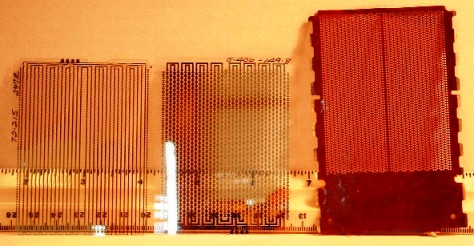
7.0 Core Memory
At the left is a 4k (4,096) bit memory plane. Initial planes like this had2,048 cores in each half (window) of the support structure. There were four wires laced through each core, the X and Y address lines, a sense line, and our inhibit line. This basic structure was used for the CP-642A, 642B, 1218s, 1219s and other computers up to the CP-901 computer. Beginning with the the AN/UYK-8, CP-890, and AN/UYK-7 the designs went to a single support window allowing the cores to be closer together thus facilitating a faster read and write time. The other key was that these systems used a three wire system. the X and Y address lines and a third wire used as the sense line during the read half cycle or the inhibit line during the write half cycle. The UYK-8 and UYK-7 projects stacked 32 planes to make up their core stack. The CP-890 was able to operate at a very conservative 1.8 microsecond cycle time. The UYK-7 and UYK-8 ran at a 1.5 microsecond cycle time. The 1830B German Navy computer also used these core stacks, continuing to operate at the 2 microsecond cycle time of the CP-901 processor.
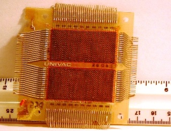
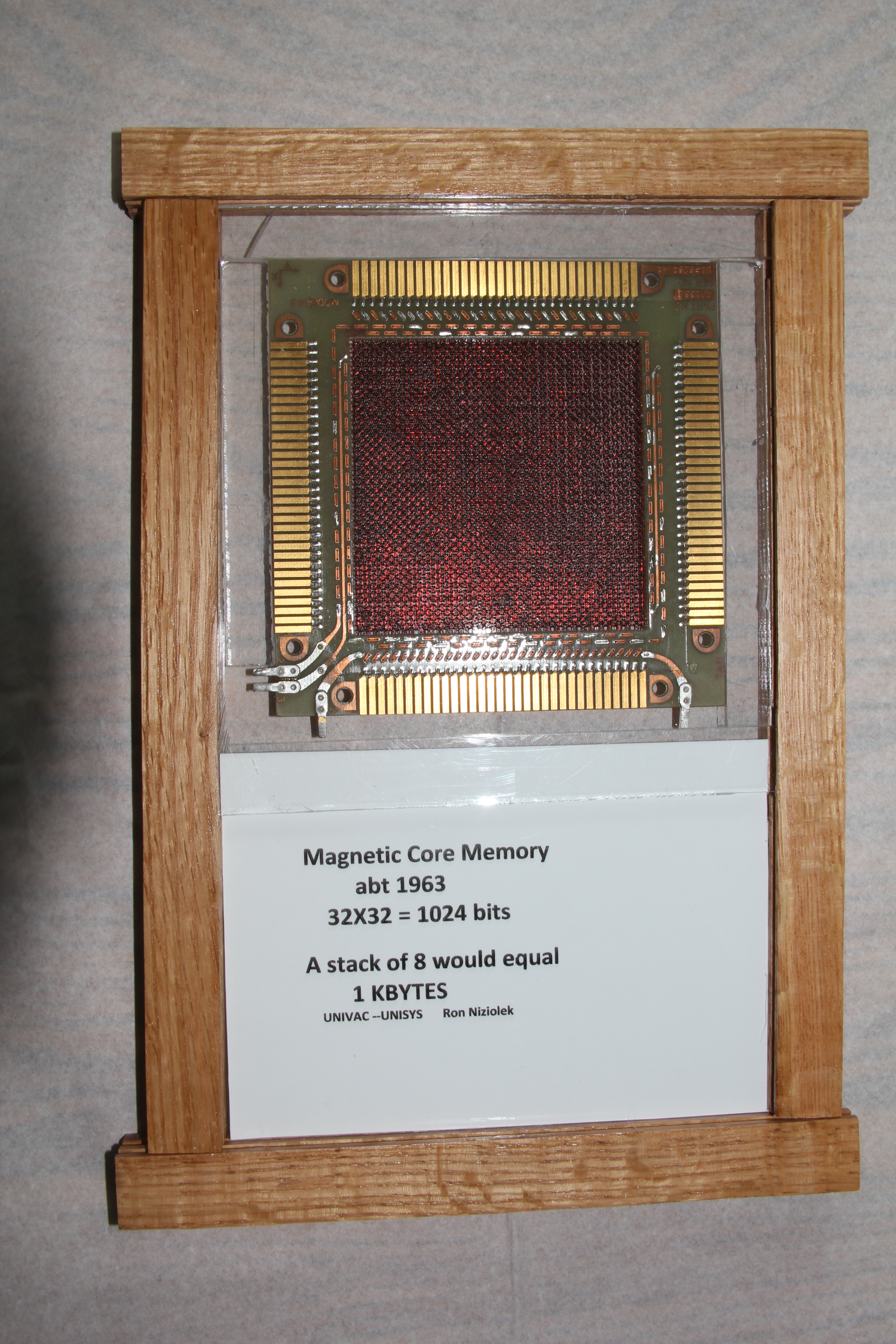 At the right is a core memory plane display submitted by Ronald Niziolek.
This 1963 design had 1024 bits in a 32 x 32 layout.
At the right is a core memory plane display submitted by Ronald Niziolek.
This 1963 design had 1024 bits in a 32 x 32 layout.
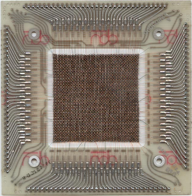 At
the left is a core memory plane from the type 1105 computer. Photo submitted by Frank Ciesla via Paul Dickson.
At
the left is a core memory plane from the type 1105 computer. Photo submitted by Frank Ciesla via Paul Dickson.
By the time we were developing the 16 bit computer line, we started to purchase core memories in a 6" x 9" x 1" module from several vendors. These had either 16k words or 32k words in a pluggable module. [lab]
8.0 Semi-conductor Memory
Many of the UNIVAC/Sperry computers made semi-conductor memories as an option. Others did a total replacement. An example of total replacement was the AN/AYK-10, type 1832 also known as the S-3A computer had an end of life replacement for the mated film memory. This was done in conjunction with the Canadian services who had a version of this computer aboard their CP-140 aircraft, http://vipclubmn.org/cp32bit.html#S3B. [LABenson]
Dick Petschauer wrote: Later the 1110 plated wire memory was also replaced with semiconductor memory but designed and manufactured at Roseville. Its size was also doubled, again by my recommendation and against that of my boss at that time, Art Schneider. Because of the high speed of the wire memory, we had to use the more expensive bipolar chips, rather than the CMOS types. I think the chip supplier was Fairchild. Later they did a “chip shrink”, a common practice to get more chips per wafer and reduce chip cost. A few months later random transient single bit errors appeared in the field. The low access time of the memory did not allow time for error detection and correction. We developed a temporary test to screen out the weaker chips in inventory. A few months later it was determined that small trace amounts of radioactive rare earth particles in the chip’s ceramic package could with time emit an alpha particle that could strike a single memory cell (basically a cross coupled transistor flip flop) and sometimes change its state. The solution was to have the manufacturer add a coating to the chip which would absorb the alpha particle. Component Engineering soon added Alpha sources to be used in chip testing and vendor qualification. http://vipclubmn.org/Articles/HISTORY1100series.pdf page 18 has more information about this application.
In this Chapter
- Introduction [left]
- Drum Memories by Lowell Benson, Larry Bolton, Dick Lundgren, & Don Weidenbach
- Braided Wire Memory by Jim Howe & Lowell Benson
- Plated Wire Memory by Bolton, Crosby, & Howe - et al.
- Bubble Memory by Lowell Benson
- Film Memory by Dick Petschauer & Lowell Benson
- Core Memory by Lowell Benson
- Semi-conductor Memory by Dick Petschauer
Chapter 45 edited 9/30/2025.
![]() |
Home, Pg 1 |
Our Legacy, Ch 1 |
People |
Locations |
Engineered |
Computers |
Systems |
Contacts and Links |
Site Map, Pg 0 |
|
Home, Pg 1 |
Our Legacy, Ch 1 |
People |
Locations |
Engineered |
Computers |
Systems |
Contacts and Links |
Site Map, Pg 0 |
Copyright ©2025, LABenson for the VIP Club. All Rights Reserved; Hosted on www.webhostinghub.com since 2011.